Description
SILICON NITRIDE TEM WINDOW GRIDS
5 nm, 10 nm, 20 nm, 50 nm, and MICROPOROUS
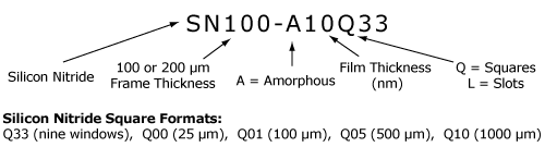
DESCRIPTION
Silicon Nitride (SiN) Microporous TEM Windows
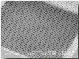
2 micron pores on 1:1 pitch in Low-Stress Silicon Nitride
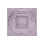
– 100 micron thick frame, fits 3 mm sample holders
– 20 nm thick Silicon Nitride film
– (1) 500 x 500 micron window
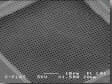
What’s NEW?
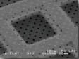
2 micron pores are patterned in 20 nm silicon nitride in a gridded pattern (see picture below) within a single 500 x 500 micron window. These microporous windows can be used for suspending a variety of thin films such as graphene as demonstrated in a recent Nature article. Additionally, these films could be used for CryoEM as well as high-tilt tomography. At 70 degree angles, the thin and beveled 100 micron silicon frame allows you to use a ~50×50 micron region within the center of the window from any rotational orientation.
100% Satisfaction Guaranteed
View the TEMwindows Silicon_Nitride brochure
TEM Windows handling Instructions
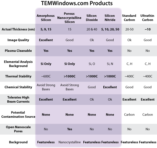
Explore how the Technical Properties of SiMPore’s Silicon Nitride films compare to other thin films
For examples of how these Silicon Nitride TEM windows can be used, please see Featuread Publications
– Competitively Priced: state of the art manufacturing processes and an expert engineering team allow us to offer Silicon Nitride solutions at competitive prices
– Plasma Cleanable: Silicon nitride grids can be vigorously plasma cleaned to remove organic contamination, unlike carbon grids
– Increased Uniformity: reduced field-to-field variability
– Tolerates temperatures >1000C: supports use in environmental TEMs where dynamic processes are observed at high temperatures
– Withstands harsh deposition & chemical conditions: provides an ideal balance of imaging resolution and mechanical strength
– Incorporates LPCVD, low-stress (~250MPa), non-stoichiometric silicon nitride: provides flat, insulating and hydrophobic surfaces


Reviews
There are no reviews yet.