Description
DESCRIPTION
Silicon Nitride (SiN) Half-Grids For Lift-Out Applications
100 micron thick frame, fits flip-stage SEM/FIB and standard TEM sample holders
– 400 nm thick low-stress Silicon Nitride film
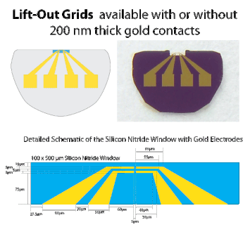
– (1) 100 x 500 micron window with the free-edge along length
What’s NEW?
Our Silicon Nitride Lift-Out TEM Windows feature a large, robust window with a freely suspended side along one length of the window, providing an easily accessed edge for sample preparation and thinning. As part of sample preparation, the low-stress Silicon Nitride can be thinned by focused-ion beam to electron transparent thickness (e.g. 50 nm or less). To prevent charging during sample preparation, we recommend coating the underside of Lift-Out TEM Windows with ~5 nm amorphous carbon by placing the grids face-down (vs. as packaged) onto cleanroom paper while in a standard carbon evaporator.
100% Satisfaction Guaranteed
LIFT-OUT GRIDS
Low-stress silicon nitride for lift-out applications
- State Of The Art: Our expert engineering and MEMS fabrication processes allow us to provide these one of a kind silicon nitride lift-out grids.
- Open Half-Grid Shape: Our Silicon Nitride Lift-Out TEM Windows feature a large, robust window with a freely suspended side along one length of the window, providing an easily accessed edge for sample preparation and thinning to electron transparency (e.g. 50 nm or less).
- Ready To Use Gold Contacts: 200 nm thick gold contacts for sample electrical biasing or heating are formatted for FIB-based sample preparation methods.
- Fit: The 100 micron thick frame and rounded half-grid shape fits flip-stage SEM/FIB holders and standard TEM sample holders.
These Lift-Out TEM Windows were developed in partnership with Dr. Matthew Mecklenburg at the University of Southern California.
Download our Application Note describing how to attach sample lamella to our Lift-Out Grids
The following featured publication describes the fabrication of our Lift-Out Grids.
Fabrication of a Lift-Out Grid with Electrical Contacts for Focused Ion Beam Preparation of Lamella for In Situ Transmission Electron Microscopy. Mecklenburg et al. (2013) Microscopy and Microanalysis. 19: 458-459.


Reviews
There are no reviews yet.